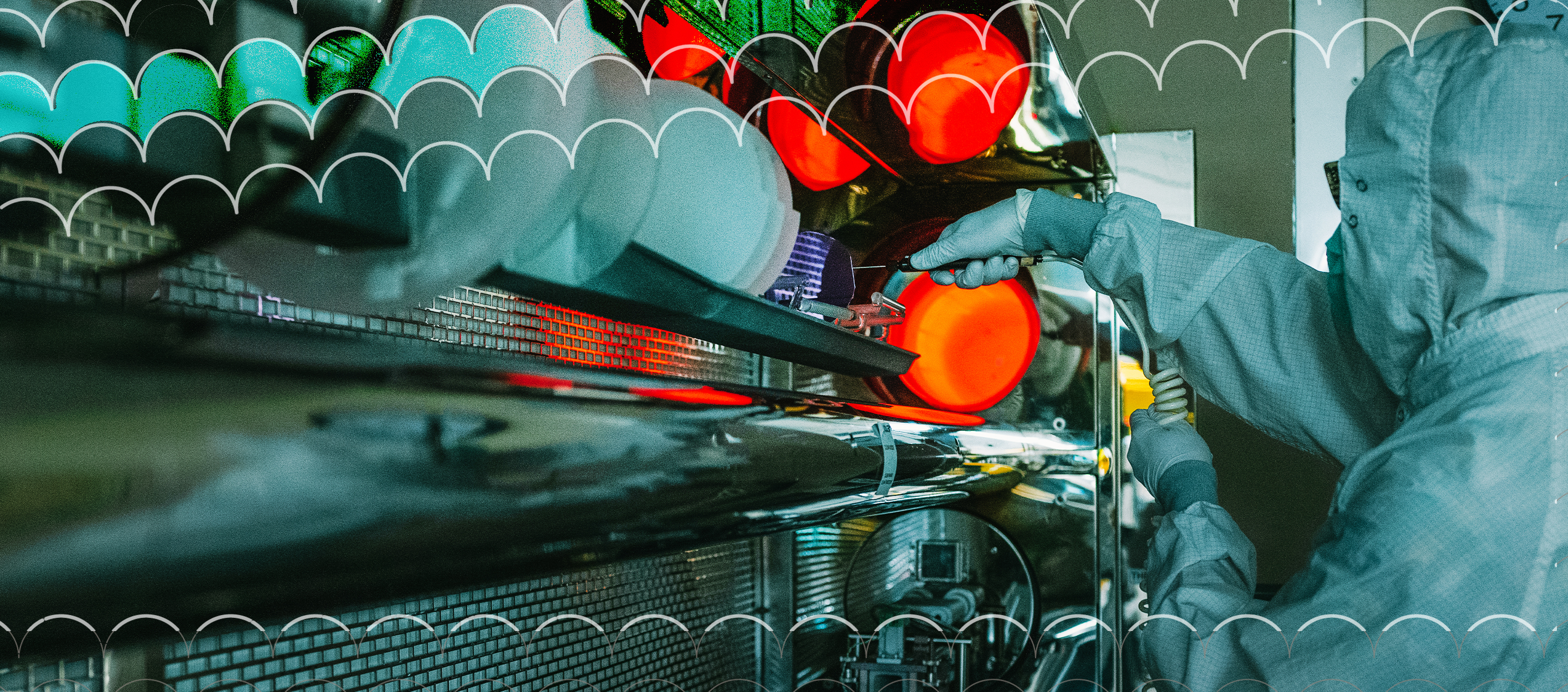
This area includes all things “nano” in EE, based on atoms, electrons, phonons, photons, and spin. Research ranges from nanofabrication of devices with new materials, to their heterogeneous integration, computational modeling, and thermal management. Projects include both fundamental aspects (e.g. what is the mobility, band gap, thermal conductivity of a new material) to practical aspects in collaboration with industry (e.g. how to translate a new fab process to industry, how to optimize new devices to exceed industrial state of the art). Examples include:
- New semiconductors for logic, memory, and sensing;
- New physics of nanomaterials, including tunneling and collective behavior;
- Insulators with high-K and low-K, high and low thermal conductivity;
- Beyond-copper interconnects, including graphene and topological semimetals;
- Transistors based on carbon nanotubes, two-dimensional (2D) semiconductors (e.g. MoS2), amorphous oxide semiconductors (e.g. ITO), wide bandgap nitrides (e.g. GaN);
- Magnetic memory, metal oxide resistive switching memory, phase change memory;
- New nanofabrication and nanopatterning techniques, including self-assembly;
- Nano- and microelectromechanical systems (NEMS/MEMS);
- Flexible devices and substrates for electronics, sensors, and energy conversion;
- Compact models, technology computer aided design (TCAD), and ab initio simulation of nanoscale devices;
- 3D-integrated circuits with layers of heterogeneous devices and interconnects;
- Nanosystems enabled by emerging technologies
| EMERITUS FACULTY | ||
|---|---|---|
| Robert Dutton | Butrus (Pierre) Khuri-Yakub | James Harris |
| Roger Howe | David Miller | Fabian Pease |
| James Plummer | Krishna Saraswat | Simon Wong |
| ALL FACULTY | |
|---|---|
| New materials, nanofabrication, and devices - View all associated faculty | |
| COURTESY FACULTY | |||
|---|---|---|---|
| Halleh Balch | Stacey Bent | Tony Heinz | David Schuster |