 |
|
To be published in "Trends in Optics 1995", ed. A. Consortini (International Commission for Optics/ Academic Press, 1995) Dense Optical Interconnections for Silicon Electronics
David A. B. Miller Ginzton Laboratory Introduction No-one can doubt the impact of semiconductor electronics over the last 30 years. Silicon integrated circuits have, for example, led to a revolution in our ability to process information. Semiconductor optoelectronics is also having a major impact, an impact particularly clear now in long-distance fiber optic communications, and in many consumer devices, such as compact disc players, and their descendants, the compact disc read-only memory (CD-ROM). Optoelectronics also seems set to be a key enabling technology in bringing high-bandwidth information services into the home through optical networks. Optoelectronics and electronics are technologies that would seem to complement one another very well for handling information. Electronics, with its ability to make sophisticated and flexible systems at low cost, dominates computing. On the other hand, optics is very good at communicating information, and has won the race for long-distance, high-bandwidth information transmission. It is also offering useful new options for information storage. Despite this complementarity, optics and electronics are perhaps not as closely intermixed as we might have imagined they would become. One problem is that optoelectronic systems have remained stubbornly expensive. Packaging individual optoelectronic devices to fibers is costly. Optoelectronic devices themselves have remained at levels of integration that are comparable to the complexity of vacuum tube circuits. The economy of scale that has driven and continues to drive silicon integrated circuits has not happened in optoelectronics. Integrated optics, for example, which integrates waveguide optics with active electrooptic or, more recently, optoelectronic devices, while still likely to be a useful technology, shows no prospect of approaching integration levels common in electronics. Without some qualitative change in optoelectronics, we are left with a rather depressing metaphor for future information processing machines. The electronic circuits become like ever denser (though increasingly sophisticated) cities, with roadways ever more crowded with information trying to get from one part of the city to the other. For transport between cities the information travels out crowded multilane highways to "optoelectronic" airports with gigantic jets. Smart Pixels There is, however, a new class of technologies emerging in optoelectronics. This class attempts to use large numbers of optoelectronic devices, usually in two-dimensional arrays, and integrate them with electronics; it is most often referred to as "smart pixels" [1] (see Fig. 1). It has become possible because of the emergence of two developments: first, high-yield optoelectronic devices capable of operating with light beams perpendicular to the surface of the device; and, second, integration technologies that allow these optoelectronic devices to be integrated very efficiently with electronics. The most difficult device problem has arguably always been in providing optical outputs (either modulators or emitters). One modulator solution is the quantum well modulator, which is the core of the class of smart pixel devices known as SEEDs (self-electrooptic effect devices) [2]. SEEDs allow arrays of thousands of fully functional optical inputs and outputs capable of operating at very high speeds. Another class is liquid crystal devices that may allow even larger numbers of somewhat slower devices [3]. Liquid crystal devices have adapted integration techniques used previously for liquid crystal displays.We may yet see large arrays of vertical-cavity surface emitting lasers (VCSELs) also integrated. SEEDs have used both monolithic integration with GaAs electronics [4], and, very recently, hybrid integration with silicon electronics using solder-bonding techniques [5].
Fig. 1. Concept of "smart pixels". Individual smart pixels will usually have optical inputs and outputs, and they will typically be arranged in a two-dimensional array. The underlying proposition of these smart pixel devices is twofold: (1) take advantage of the many communications advantages of optics (including many currently not exploited in fiber optic systems) together with all of the processing abilities of electronics to allow higher performance systems; (2) avoid the high current cost of each optoelectronic "connection" by working with large arrays of such connections at once. To exploit such smart pixels will require advances in two areas other than the device and integration technologies. First, we need optical technologies that can work with arrays of light beams. Second, we need systems architecture concepts that can exploit such array parallelism. Some switching architectures have been investigated and demonstrated already [6] [7]. Below we will look more closely at some of the key features of silicon technology and of optics, and discuss one recent technology, the hybrid SEED [5], in more detail. Silicon Technology The number of transistors on a silicon circuit has approximately doubled every 18 months for the past 2 decades, and it currently looks likely that this trend will continue [8], perhaps even for 15 years or more. Current electronic logic chips can have millions of transistors, and memory chips can have even more. It may even be that this progress has now become self-fulfilling, with different manufacturers using these predictions to know where they should be at a given time in the future to be competitive. The investment in delivering such future technology is certainly large, and no other technology seems likely to compete with electronics in the immediate future as far as complexity is concerned (though biological systems are an existence proof that systems much more complex and sophisticated than silicon are possible). Certainly optics has no way of matching such complexity, and no current prospect of an investment large enough to allow it to catch up even if it had a viable approach. With all this advance of silicon, is there any role for optics? Will it not always be behind? Will optical machines not always be relegated to special purposes, to be overtaken by the advancing general purpose silicon? We could, of course, argue that optical devices may be able to operate with performance silicon cannot beat, such as ultrafast nonlinear optical logic gates, but it is difficult to imagine how we could make systems with sufficient complexity to rival silicon for performing mainstream information processing tasks, and so optics appears to be relegated again only to special purpose tasks. It is also likely that silicon devices as we know them will run into physical limits as miniaturization continues, but it is by no means clear that optics offers the generation beyond the tiniest silicon device. Silicon electronics has its weaknesses, however, and there are many related to the difficulty of interconnections. Electrical interconnections are dominated by problems of classical electromagnetics. Such problems do not necessarily scale well as silicon devices improve. They are connected with classical resistance and capacitance of lines, and with Maxwell's equations, phenomena that have little to do with silicon devices themselves. Furthermore, smaller silicon devices also tend to be able to run faster, and trying to exploit this increased speed only makes the problems of interconnections worse. Suppose, for example, that, as we made the silicon devices smaller, we also scaled down the electrical wiring on the chip, scaling down both the widths and the thicknesses of the lines. On a silicon chip, the time taken to send information is essentially limited by the time taken to charge up the electrical line on the chip. Halving the width and thickness of the metal lines would multiply the resistance by a factor of 4 for a given length; the capacitance would remain the same (the line would be half as wide, but the dielectric would be half as thick), and hence the resistance capacitance (RC) product for a given length of line would have gone up by a factor of 4. At best, we might argue that the line only needs to be half as long since the transistors are half the size also, but even then the RC product remains the same. Not only is the line no faster than it was before, but the smaller transistors can probably run about twice as fast, so the issue of the delay of the interconnect line is becoming even more of an impediment to exploiting the capability of the silicon. Of course, silicon technologists are well aware of such problems [8], and are doing their best to minimize them. For example, metal line thicknesses will likely not scale down with the width of the lines, and attempts will be made to reduce dielectric constants and metallic resistances. There can be little doubt that the interconnections will more and more limit the capability of silicon systems as silicon itself becomes more capable. Indeed, circuit architecture innovations to compensate for long interconnects and higher clock speeds are seen as one of the highest priority research needs in silicon technology [8]. Yet another set of problems arises as the signals leave the chip. For low speeds (e.g., less than 10 MHz) we can often think of interconnections as simple wires, with signals traveling "instantaneously" from one end to the other. But at high speeds (e.g., > 100 MHz), we must treat the signals as waves on transmission lines. Impedances must be matched to avoid reflections, terminating resistors (usually about 50 ohms) must be used, and associated low-impedance line drivers (with correspondingly high power dissipations) must be constructed. Cross-talk between lines becomes a more significant issue because the lines become progressively more efficient broadcasting and receiving antennas at higher frequencies. Signals become distorted because of the finite frequency response of the lines. The lines also become lossier at higher frequencies because of the skin effect (which forces electrical conduction into an ever thinner layer near the surface of the metallic conductors at higher frequencies). Synchronization of the arrival of signals also becomes progressively harder. Again, though engineers become very adept at minimizing the effects of these various issues, they are problems that only become progressively worse as the silicon circuits become larger and faster.
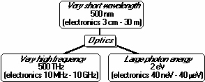
Fig. 2. Fundamental difference between optics and electronics for communication, expressed in terms of wavelength, frequency and photon energy. Reasons for Optical Interconnections There are many reasons why optics can help with interconnecting information, and only a few of these are exploited at the moment. All of the potential advantages of optics in this regard come from the same fundamental difference between optical and "base-band" (i.e., radio frequency) electromagnetic waves. This difference can be expressed either in the higher frequency, the shorter wavelength, or the larger photon energy of optics, all three of which are different manifestations of the same difference (Fig. 2). High frequency of light The high frequency of light has several consequences. (a) The carrier frequency of light is so much higher than any frequency at which we can modulate that such modulation makes essentially no difference to the propagation of light, at least over the distances within machines. Hence there is no frequency-dependent loss or frequency-dependent crosstalk when using light as the information carrier (whether in fibers or free-space) within machines. This is in strong contrast with wires, where such frequency-dependent loss and crosstalk become rapidly worse at high frequencies. There may well, of course, be loss and crosstalk with optics, but they get no worse at high speeds.
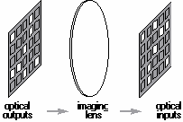
(b) There are situations in optics where we must match impedances, as for example when we transition from propagating in air or glass into a semiconductor material. Because the modulation bandwidth we use is so narrow compared to the carrier, we can use very simple "resonant impedance transformers" - dielectric anti-reflection coatings. There is no comparable simple impedance transformer we can use for broad band radio-frequency waves. Short wavelength of light The short wavelength of light leads to the following benefits. (c) Because the wavelength of light is so small, we can make waveguides that are much larger in cross-sectional dimensions than the optical wavelength (e.g., a 10 micron diameter core in an optical fiber is much larger than the approximately 1 micron wavelength of light). As a result, we can guide the waves entirely with dielectrics, and hence have very low loss propagation. In purely electrical systems, the radio-frequency wavelengths are often comparable to or larger than the entire system, and certainly larger than most current integrated circuits. To guide the information to where we want it to go, we need to use the very large effective dielectric constants of metallic conductors. Since these conductors are not perfect, we sustain losses. (It is tempting to think that it is electrons that carry information in wires, but this is not really correct. The proof is simple - the information does not travel at the electron velocity, but rather at some fraction of the velocity of light in low-loss transmission lines or at an effective velocity set by line resistance and capacitance in the dissipative propagation found on, for example, connections within integrated circuits.) (d) The small wavelength allows us to contemplate information flowing on and off chips without the use of waveguides. We can instead image many light beams from one chip to another (Fig. 3). Such imaging is only possible because the wavelength is so much smaller than the systems we are interested in. The smallest region we can image in practice is about one wavelength in size, and so attempting to image "base-band" electromagnetic waves would typically only allow one interconnection out of a system - essentially a radio transmitter. With optics, however, it is routine to image 1000's of "outputs" from one plane onto 1000's of "inputs" on another with a single lens. Despite the fact that all of the beams may overlap at the lens, the lens separates out all of the information again to image the multiple beams at the receiving "inputs". Optics therefore allows very large numbers of connections from one plane to another through "free space". An incidental benefit is that all of the connections in such imaging-based systems are automatically very well synchronized with one another, hence avoiding another practical problem of "signal skew" common in electrical systems. Another related consequence is that it is possible to make very global interconnect topologies (such as so-called "perfect shuffles") in which many of the "beams" cross through one another. Such patterns can be useful for operations such as telecommunications switching fabrics and fast Fourier transforms.
Fig. 3. Concept of imaging arrays of outputs on one plane to arrays of inputs on another. Large photon energy of light The fact that the photon energy of light is so large has two consequences, one already extensively exploited, and another that has only relatively recently been understood. A key physical point about light's large photon energy is that light is both generated and detected quantum mechanically, not classically - for example, detection of light in practice involves counting photons, not measuring electric field amplitudes. (e) Detecting photons allows us to generate "d.c." currents and voltages without any direct electrical connection with the light source. In other words, optical interconnects give us perfect electrical isolation between two circuits, and make the absolute voltage levels in the different circuits irrelevant. This solves an important problem in electrical systems, and is exploited extensively in so-called "opto-isolators", which usually contain a light-emitting diode (connected to the "transmitting" circuit) and a photodiode (connected to the "receiving" circuit). (f) Use of optical emitters or modulators and photodiodes also fundamentally enables us to avoid the problems of the low impedance of electrical transmission lines [9]. The low impedance of electrical lines (typically 50 ohms) is a direct consequence of the low impedance of free space (377 ohms) and the fact that transmission line impedance only scales logarithmically with the conductor sizes. A related problem is that all electrical lines have about 1 pF/cm or more capacitance, and there is little that can be done to reduce that either. A key consequence of such low impedance and high capacitance is that line driver circuits have to be made, and these unavoidably consume relatively large amounts of power (e.g., 10's to 100's of mW per high speed electrical line). The use of transmission lines becomes unavoidable at high clock rates (e.g., > 100 MHz or so) off chip. The resulting power dissipation and use of chip area for drivers is a significant issue in chip design when high data throughput is required. The reason why optics can avoid the low impedance problem is that the voltage generated in a photodetector bears no particular relation to the classical "voltage" in the light beam. It is quite possible, for example, to generate 1 V in a photodetector from a light beam with 600 microvolts of classical voltage [9] - a consequence, fundamentally, of the photoelectric effect. This particular benefit has not historically been exploited in practice because the optical sources have always consumed more power than a 50 ohm resistor anyway, so there was no power savings, and the driver problem was, if anything, worse than that of an electrical line. The emergence of quantum well modulator technology has, however, led to quite practical low-power optical output devices that can demonstrably send digital signals from chip to chip with substantially less power (e.g., < 10 mW total dissipation at 150 Mb/s) than electrical connections [10]. Other approaches, such as low threshold lasers, may be able to offer similar benefits. This feature of optics is likely to be particularly important for large arrays of optical inputs and outputs, as in smart pixels, and may allow much larger amounts of information to be sent on and off chips optically than is practical electrically. The various features of optics for interconnections discussed above clearly address many of the problems that are being encountered more and more in making electronic information processing systems. These features come directly from the differences in the physics between optics and electronics. The fact that the beneficial features of optics are so firmly rooted in the physics gives us reason to believe that optics will eventually be used extensively in interconnection in electronic systems. Hybrid SEED Technology A technology that allows easy conversion between electronics and optics and vice versa, and that allows large numbers of devices, is crucial for the more radical concepts like "smart pixels". Such a technology should ideally fit well with silicon electronics as it exists, without requiring any substantial changes to that technology, and should be capable of operating at the speeds and voltages of silicon circuits. Arguably the first such technology to emerge, and the most advanced at this time, is the hybrid SEED (self-electrooptic-effect device) [5]. The hybrid SEED relies on quantum well diode modulators [11]. Quantum wells, made of alternating very thin (e.g., 10 nm) layers of two different semiconductor materials, show a large change of optical absorption when an electric field is applied perpendicular to the layers [12]. If we put many (e.g., 50 - 100) such layers inside a diode, reverse biasing the diode gives us a convenient and low-power way to apply the necessary field. Such diodes need only be a few microns thick overall yet still have sufficient change in optical transmission to make useful modulators. This allows two-dimensional arrays of such diode modulators to be made using standard semiconductor growth and processing techniques. The modulators are very fast, limited in practice only by the electrical drive circuits and parasitics, and can operate with moderate voltages (e.g., 5 V). The modulator diodes also function as good photodiodes, so the same device can be used for optical inputs and outputs.
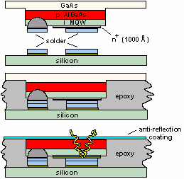
Fig. 4. Illustration of the hybrid solder bonding process used to bond arrays of quantum well diode modulators and detectors to silicon CMOS circuitry in the hybrid SEED process. With the final removal of the epoxy, individual modulators are left connected to the silicon circuitry in a two-dimensional array. In the hybrid SEED, arrays of such quantum well diodes are made, with reflecting metal on the top. Then the array is turned over and solder-bonded to the silicon circuit, and, as shown in Fig. 4, the entire substrate material is removed chemically from the quantum well diodes to leave isolated diodes bonded to the silicon circuit. The resulting array can be used as reflection modulators or photodetectors, depending on the silicon circuits to which they are connected. The use of reflection modulators is convenient since it means that light does not have to pass through the silicon circuits, so conventional silicon circuit mounting can be used, and the double pass of the light beam through the modulator increases the amount of modulation of the light beam. The only additional processing needed of the silicon circuit is to deposit some metals and solder. This can be done after the usual fabrication of the silicon wafer, and no change is required in the usual fabrication process. As a result, this technique can be used with silicon circuits from any fabrication process. Fig. 5 shows a picture of a silicon circuit with attached quantum well diodes. In this case, the diodes are about 15 x 40 microns in area, and the solder bonds are about 15 x 15 microns in size. It is interesting to note that these optical input and output "pads" are much smaller than the electrical bonding pads used on chips to carry signals electrically on and off chips.
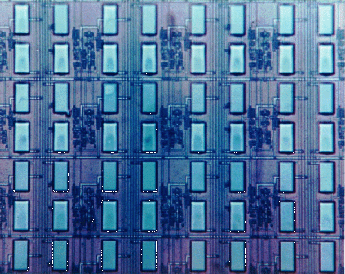
Fig. 5. Picture of part of a hybrid SEED chip. The quantum well diodes are the regular array of rectangles, and are approximately 15 x 45 microns in area and a few microns thick. Underneath is active silicon circuitry. More than 1000 of these quantum well diodes have been successfully bonded to a silicon chip [5]. Operating circuits have been demonstrated with this approach, including circuits with complex functions [13] and optical input and output receiver and transmitter circuits [14] running as fast as 700 Mb/s. These 700 Mb/s results were obtained using 0.9 micron feature size silicon, which is remarkable because such silicon with electrical inputs and outputs is normally run at clock rates of about 100 MHz; the optics may be allowing much faster operation than would normally be contemplated in purely electrical systems. An important point about this hybrid approach is that, as silicon electronics gets better, the optoelectronic systems based on this approach get better also. We expect still to be able to hybridize to future generations of silicon technology with smaller feature sizes and faster transistor performance. It is also reasonable to expect that in the future even larger numbers of optoelectronic devices can be integrated. Challenges There are many challenges in trying to take advantage of optics in information processing machines. In the evolutionary approach of gradually substituting optical fiber for copper wire down to ever shorter distances, cost is perhaps the major issue. Beating electrical wiring on cost is hard; though it has its technical limitations, it does what it does for low cost, and it is difficult to compete when trying to substitute directly for it with similar performance. The approach we have discussed here is, however, more revolutionary. Rather than trying to substitute for copper or aluminum wiring in systems already optimized around the constraints of such a technology, the "smart pixels" approach would attempt to generate new kinds of systems that can directly exploit the many abilities of optics. This approach raises many challenges. The first kind of challenge is the more obvious but real technical one of delivering the devices and systems components at low enough cost and high enough performance. Device technologies, such as the hybrid SEED, are emerging, and appear to have good chances of delivering impressive performance. Specific areas of work for the hybrid SEED will be in continuing to make larger numbers of devices in arrays, and to progressively reduce the operating voltage to track the expected reduction in the voltages in electronics. An area that is still in need of innovation and more practical technology is that of optics and optomechanics for arrays of light beams. Substantial systems have been built, proving that array optics and optomechanics is possible - for example, one system operated successfully with more than 60,000 light beams [6]. Such systems need to evolve from a "brass-board" level that allows systems prototypes, towards practical, low-cost, manufacturable systems. The SEED technology, being based on modulators, also needs external laser power sources. It has usually been run using diode laser sources, and these are likely to continue to improve, though SEED systems usually want good wavelength stability and output power. Recent developments in diode-pumped solid state lasers are also promising here, including techniques that allow short pulse generation [15]. The use of external lasers has the significant system advantage of allowing the entire system to be "clocked" globally by clocking one laser, and the use of short pulses has several additional advantages, including very well defined "clock" pulses, and also ways of reducing the operating energy of systems [16]. There is even a possibility of using such short pulses to make convenient ways of working with multiple wavelengths at once [17]. The second kind of challenge is a more subtle one - we need to devise the classes of systems that can best exploit what optics can do. We should not underestimate the extent to which current electronic systems are optimized around the particular problems and benefits of electrical connections. For example, it is not unusual for a high-performance electronic chip to have its area and power dissipation devoted approximately equally to each of the three functions of (i) input/output, (ii) clock distribution, and (iii) logic and memory circuitry; such a balance is likely not accidental, and reflects the intrinsic optimization done by the chip designer. Optics can likely substantially impact both the clock distribution and the chip input/output, hopefully allowing a higher system performance overall. At the chip level, therefore, and also likely at other levels in the system (such as the board-to-board level), there are many opportunities for optics to allow a re-optimization of the system design for higher performance overall. It is, however, important to be doing the research now on how we might do this optimization to take advantage of optical technology as it becomes available. Another important aspect of this second challenge is that the optically enhanced systems must interface to the existing electronic world; they must make this interface in two ways, both physically and in a more subtle way that we can refer to as "hierarchically". The physical interface difficulty is what we can call a "fire-hose" problem - a reference to the metaphor of attempting to drink from a fire hose pumping out vast quantities of water at high pressure. Optical systems may allow us to communicate vast amounts of data in and out of a chip, but this is of little use if we have no way of feeding this "fire-hose" of data into the chip or of handling a similar "fire-hose" of data out of it. There are several kinds of systems that do solve this problem. One is the kind of system that we might encounter in telecommunications switching, where we can make up the large fire-hose of data by bringing together a large number of smaller pipes of data, one pipe from each input line to the switching system (with a similar inverse arrangement at the output), with each pipe being carried on an optical fiber into an array of fibers that might be imaged onto the chip. Another kind of system would be one in which the internal data rate might be higher than the overall input and output rates. One such example would be a processor for multiplying vectors by a relatively fixed matrix - the input and output would only be vectors (one-dimensional parallelism), but internally the parallelism could be two-dimensional. Examining the architectural possibilities here should be a subject of research now. Information processing machines are built and operated using a very sophisticated hierarchy of technologies and levels of abstraction. At one extreme, we have device physics and device technology. At the other extreme is the human interface with perhaps a computer screen or a telephone. In between, we find algorithms, logic design, assembler language, high-level computer languages, backplane architectures, bus protocols, and many other concepts. Here we come to the "hierarchical" challenge for the use of optics. The development of each of these levels in the hierarchy has required substantial investment. If we come along with a concept for a processor that requires that we change many levels in this hierarchy, it will be very difficult to implement because it will be expensive to replace all of those many levels. It is already clear that, even at the hardware level, the use of optics requires that we change several levels of the hierarchy; we must try in our architectural concepts to avoid changing many more if at all possible, at least initially. Technologies such as the hybrid SEED help in that they are intrinsically very well linked to conventional electronic technologies. At higher levels, this difficulty of changing levels in the hierarchy suggests that we might look at optically assisted processors as "co-processors", processors that are addressed and controlled at a higher level by conventional processors, but that perform specific tasks or "instructions" particularly efficiently. Examples of this approach in the electronic world are math co-processor chips as used in personal computers, and digital signal processor chips. Optically assisted co-processors might include signal processing functions (including, for example, Fourier transforms and correlations), switching functions (such as a high performance switching fabric for telecommunications switching or interconnection multiple processors), or matrix math functions (such as inversion and multiplication). A key difference of the emerging smart pixel approach compared to many previous optical approaches is that the smart pixels can operate digitally, thus avoiding problems of limited analog accuracy, and in general their digital format and use of existing silicon technology helps a lot in reuse of existing levels of the hierarchy. Prognosis When will we see such two-dimensional array optics being used in real machines? Of course, that is a difficult question to answer, and depends on many things, some technical and some not. One possible driver is machines that must handle very large throughputs of data. We could speculate that by the year 2000 we may need to have telecommunications switching machines with capacities as large as 1 Tb/s [18]. It may also be that large database machines will approach similar capacities at this time, and perhaps also specialized image processing machines. Certainly, if one machine of this class is produced it is likely that machines for other purposes will try to exploit the technology. Machines with capacities of about 100 - 200 Gb/s are being researched now based on electrical technology. Such machines typically consist of many cabinets, with very large numbers of electrical cables connecting the cabinets. It is probably possible to make machines with 1 Tb/s capacity this way, but the intercabinet wiring problem is likely to be substantial, and it is not clear that this approach can continue scaling as problems such as switching may require [18]. Hence there may be a real opportunity for optics. If two-dimensional optics for interconnection comes into first serious use by about the year 2000, then by the year 2010 we might expect to see volume use, with cheap optical power, and cost-reduced optomechanics. By that time systems would likely be designed so that optics is essential to get the architectures and performance customers need. Of course, we could argue that such predictions, in addition to being speculative, are so distant as to be useless. In fact, however, if we are to meet such "deadlines" of 2000 and 2010, history suggests that we had better be doing the research now - 15 years is a short time to turn a new paradigm into a practical reality with a mass market. Too often in the past we have seen promising schemes for "optical computing" defeated because of the continuing improvement in silicon technology. In the case discussed here, improvement of silicon technology only helps the capabilities of these optoelectronic systems. Optics here is not competing with silicon - instead it is competing with aluminum and copper, which are much more slowly moving targets. Indeed it may be the optoelectronics, through its ability to provide dense, high speed and low power interconnection, that allows us to exploit the real capabilities of silicon electronics. References [1] See for example, Special Issue on Smart Pixels (ed. S. R. Forrest and H. S. Hinton), IEEE J. Quantum Electron. 29, No. 2, February 1993 |